
Junction Field Effect Transistor
STRUCTURE OF JFET
A junction field effect transistor (JFET) is a three terminal . Semiconductor device in which current conduction is by one type of carrier. I.e, electrons or holes. In a JFET, the current condition. Is either. By electrons and holes and is controlled by means of an electric field between the gate and the conducting channel of the device. The JFET has high input impedance and low noise level.
CONSTRUCTION:
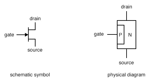
A JFET consists of a P-type or N-type silicon bar containing two PN junctions at the sides as in fig.The bar forms the conducting channel for the charge carriers. If the bar is of p type it is called N channel JFET and if the bar is of the p type it is the P channel JFET. The two PN junctions forming diodes are connected internally and the common terminal called gate (or gate diode) is taken out. Other terminals are source and drain. Thus, a JFET has the essentially 3 terminals get source and drain. the gate is reverse biased. this is the normal way of JF ET connection. the drain and source terminals are interchangeable.
Operation:
- when a voltage VDS is applied between drain and source and voltage on the gate tis zero (VGS =0)the two PN junctions at the sides of the bar establish depletion layers. The electronic flow from source do drain through the channel between the depletion layers. The size of these layers determine the channel with and hence the current conduction through the bar.
- when a reverse gate voltage V GS is applied between gate and source, the depletion layers width is increased. This Reduce the channel width and thereby increased. This reduces the channel width and thereby,. Increasing the resistance of N type bar. Consequently, the current from source to drain is reduced. On the either hand if the reverse get voltage is decreased the width of the Depletion layers also decreases and channel resistance decreases and this the channel width and current conduction increases.
- Thus the current conduction can be controlled by the application off voltage on the gate. for the reason this device is called field effect transistor and is a voltage controller device.
APPLICATION OF JFET:
•Used as buffers in measuring equipment receivers and other general purpose devices.
•Used in RF amplifiers used in FM tuners and Communication equipment
•used in mixer circuit In FM and TV receivers and communication equipment
• used in in cascade amplifiers in measuring and test equipment.
•used in hearing aids and inductive transducers.
•used in oscillator circuits.
•As the physical size is small it finds use in digital circuits in computers large scale integration (LSI) and memory circuits.


Recent Comments