
R and RC Triggering of SCR
R AND RC TRIGGERING CIRCUITS
AIM:
To design and setup R and RC triggering circuits for a half controlled rectifier for different firing angles and draw relevant wave forms.
EQUIPMENTS AND COMPONENTS REQUIRED:
| Sl No | Apparatus/Tool | Specification | Quantity |
| 1 | SCR- | ||
| 2 | Ammeters- | ||
| 3 | Power Supply- | ||
| 4 | Wattage Resistors- | ||
| 5 | Voltmeters- | ||
| 6 | Potentiometers | ||
| 7 | Capacitor | ||
| 8 | SCR | ||
| 9 | Transformer | ||
| 10 | Bread Board |
THEORY
R Firing circuit:
Figure shows the most basic circuit. R2 is the variable resistance. Rb is the stabilizing resistance. If R2 is zero, gate current may flow from source through R1, D and gate to cathode. This current should not exceed maximum permissible gate current Igm. R1 can therefore be found from the relation (Vm/R1) ≤ Igm. The function of R1 is to limit gate current to a safe value, as R2 is varied. Resistance Rb should have such value that maximum voltage drop across it does not exceed maximum possible gate voltage Vg. This happens only when R2 is zero. Under these condition . As resistances R1, R2 are large, gate trigger circuits draw a small current. Diode D allows the flow of current during the positive half cycle only i.e., gate voltage is half wave DC pulse. The amplitude of this DC pulse can be controlled by varying R2. The potentiometer setting R2 determines the gate voltage amplitude. When R2 is large, current I is small and voltage across Rb is Vg = I x Rb. As Vg is less than Vgt SCR will not turn on. Trigger circuit consists of resistance only. Vg is therefore in phase with source voltage Vs. Adjust R2 in such a way that Vg = Vgt at different firing angles depending upon instantaneous values of input voltage. When R2 is large enough to such that Vg become equal to Vgt only at peak value of output voltage, corresponding firing angle will be 900. The resistance triggering cannot give firing angle beyond 900.
CIRCUIT DIAGRAM:
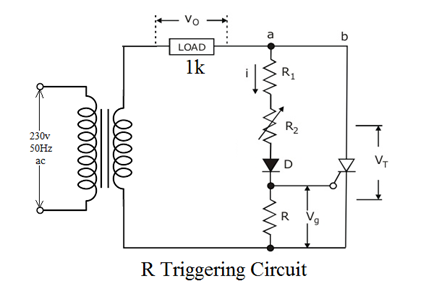
Design:
- When R2 is minimum, Ig will be maximum. Igmax = 100 mA
- Therefore = 170 Ω. (Use 220Ωstd.)
- When R2 is maximum, current will be minimum and voltage drop across Rb will be maximum and it should not exceed Vgm
- Vgmax = 2.5 V, Vm = 12√2 V
- When R2 = Max, Vgt = 0.8 V, Vm = 12√2 V
- R2 = 0.447 Ω (Use 1K pot std)
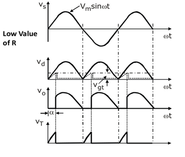
Sample Wave forms:
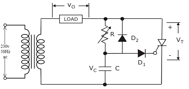
RC Firing circuit:
Fig.2 shows the RC half wave triggering circuit. By varying the value of R, firing angle can be controlled from 00 to 1800. In the negative half cycle capacitor C charges through D2 with lower plate positive to peak supply voltage Vm at ωt = 900. During the period ωt = -900 to ωt = 00, Vc may fall from –Vm at ωt = 900 to some lower value at ωt = 900. As the SCR anode voltage passes through zero and becomes positive C begins to charge through variable resistance R from initial voltage. When the capacitor charges to positive voltage equal to Vgt, SCR is fused and after this capacitor holds to small positive voltage. D1 is used to prevent breakdown of cathode to gate through D2 during negative half cycle. The SCR will trigger when Vc= Vgt+ Vd. At the instant of triggering VC is assumed constant.
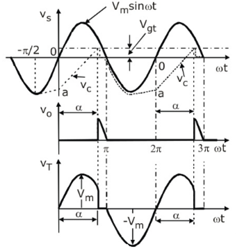
Sample Wave forms:
PROCEDURE:
Set up the circuit on breadboard. Turn on the SCR by adjusting triggering pulse. Note down the maximum and minimum firing angle. Observe the wave forms corresponding to each firing angle.
RESULTS:
The circuit is setup and the wave forms for various firing angles are observed and plotted.


Recent Comments