
Digital Triggering Circuit of SCR
DIGITAL TRIGGERING CIRCUIT
AIM:
To design and set up a digital triggering circuit, suitable for triggering a single phase half wave controlled rectifier.
EQUIPMENTS AND COMPONENTS REQUIRED:
| Sl No | Apparatus/Tool | Specification | Quantity |
| 1 | SCR, TTL IC 74121 | ||
| 2 | Ammeters- | ||
| 3 | Power Supply- | ||
| 4 | Wattage Resistors- | ||
| 5 | Voltmeters- | ||
| 6 | Potentiometers | ||
| 7 | Capacitor | ||
| 8 | SCR, | ||
| 9 | Transformer | ||
| 10 | Bread Board |
THEORY
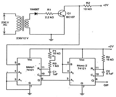
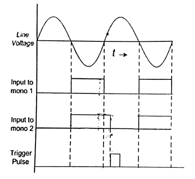
The actual firing circuit of a digital firing circuit suitable for triggering a single phase half wave controlled rectifier is shown in figure. The supply voltage is stepped down to an appropriate value and fed to the base of transistor Q1. The Transistor outputs a square wave in synchronism with the ac input. The square wave is fed to the monostable-1 (TTL IC 74121) which is positive edge triggered. At the positive going edge of the input signal, the output of monostable-1 becomes high. Then after a time delay of Td1 = 0.7R1C1, the output of monostable-1 becomes low. Td1 can be varied from 0 to T/2 by varying the resistance R1. The output of monostable-1 is the triggering input to monostable-2, which is negative edge triggered. So in every positive half cycle of the supply voltage, monostable-2 is triggered to the high state at a delay time of Td1. It is designed to remain in the high state for delay time Td2 which is sufficient to turn on the SCR.
The output of monostable-2 is amplified and applied to the gate of SCR after isolation. By varying the resistance R1, the firing angle can be varied from 0 to 180o. In the pulse amplifier and isolation block, the transistor is for pulse amplification and the pulse transformer is for providing isolation between power circuit and firing control circuit. The diode placed across the secondary of the pulse transformer protects gate of the thyristor from large reverse voltages. The diode in series with the gate prevents any leakage current flowing in the gate circuit during transistor conduction. The diode placed across the primary of the pulse transformer protects the thyristor from over voltages.
- Time delay of monostable-1 is given by
- Td1 = 0.7R1C1
- Maximum time delay, Td1 (max) = 0.7 R1maxC1
- Since maximum time delay is 180o,
- Td1 (max) = T/2, where T is the time period of the ac supply.
- Width of output pulse Td2 of monostable-2 should be sufficient to turn on the SCR.
- Td2 = 0.7R2C2
- R2 = Td2 / 0.7C2
CIRCUIT DIAGRAM:
Sample Wave forms:
PROCEDURE:
The circuit is set up, supply is switched on. Waveforms at different points are observed on the CRO. The firing angle is varied by varying the resistance R1. For different firing angles, the above waveforms are observed.
RESULT:
A digital firing circuit has been designed and set up for triggering a single phase half wave controlled rectifier.


Recent Comments