
TTL Characteristics
TTL CHARACTERISTICS
AIM:
To plot the sourcing, sinking and transfer characteristics of a TTL NAND gate and to measure sourcing and sinking current.
MATERIALS AND TOOLS REQUIRED:
Digital trainer kit, IC 7400, ammeter, voltmeter, potentiometer, dc supply etc.
THEORY:
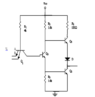
The internal circuit diagram of a basic TTL NAND gate is shown in figure. If any of the input is in low level, the output will be in high level. If any of the input is in low level, the output will be in high level. If any of the input of the NAND gate is low, Q2 and Q3 will be turned off and Q4 will be turned ON to give a logical 1 output.
Circuit Diagram:
PROCEDURE:
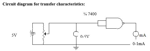
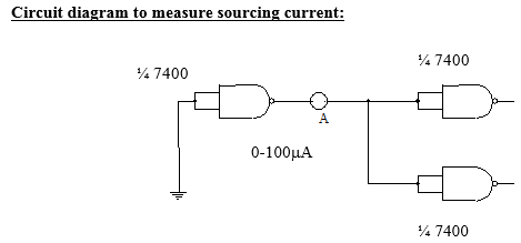
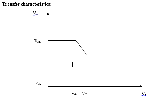
Test all the components and IC packages using digital IC tester. Set up the circuit t87o measure sourcing current. Ensure that the gate output is in logic 1. Take the reading from ammeter. Set up the circuit to measure sinking current. Ensure that the gate output is in logic 0. Take the reading from ammeter. Set up the circuit to measure transfer characteristics. Vary the input voltage from 0 to 5V. Take the voltmeter readings. Draw the characteristics with Vi on X-axis and V0 on Y-axis. To display transfer characteristics on CRO, feed a 5V triangular waveform to the input of the gate. Feed the signals to channel A and B as shown in the figure and turn time base knob of CRO to transfer characteristics position.
RESULT:
- Logic swing = ………..
- Transition width = …………
- High level DC noise margin = …………
- Low level DC noise margin = …………


Recent Comments