
Microcontroller & Programmable Logic Controllers
Microcontroller & Programmable Logic Controllers
- Write any six features of 8051 micro controller?
- All peripherals are integrated into a single chip, the overall system cost is very low.
- Simple to integrate in any electronic device.
- Simple architecture.
- Low computing power.
- The product is of a small size as compared to the microprocessor based systems and is thus very handy.
- 4KB bytes on-chip program memory (ROM)
- 8-bit bidirectional data bus & 16-bit unidirectional address bus.
- All the peripherals are integrated with a microprocessor, the system is more reliable.
- 32 general purpose registers each of 8-bit
- 16-bit program counter and data pointer
- All the features are available in a 40 pin package as in an 8 bit processor.
2. Sketch the architecture of 8051?
The 8051 Micro controller is an 8 – bit i.e. it can read, write and process 8 – bit Data. CPU is the brain of any processing device of the micro controller. It monitors and controls all operations that are performed on the Micro controller units.
ALU or Arithmetic Logic Unit, as the name suggests, performs 8 bit Arithmetical and Logical Operations over the operands held by the temporary registers TMP1 & TMP2.The 8051 contains 34 general purpose or working registers. Two of these Register A (Accumulator ) and B.
Accumulator (ACC): The immediate result is stored in the accumulator register for next operation.
B register: It is a register just for multiplication and division operation which requires more register spaces for the product of multiplication and the quotient and the remainder for the division.
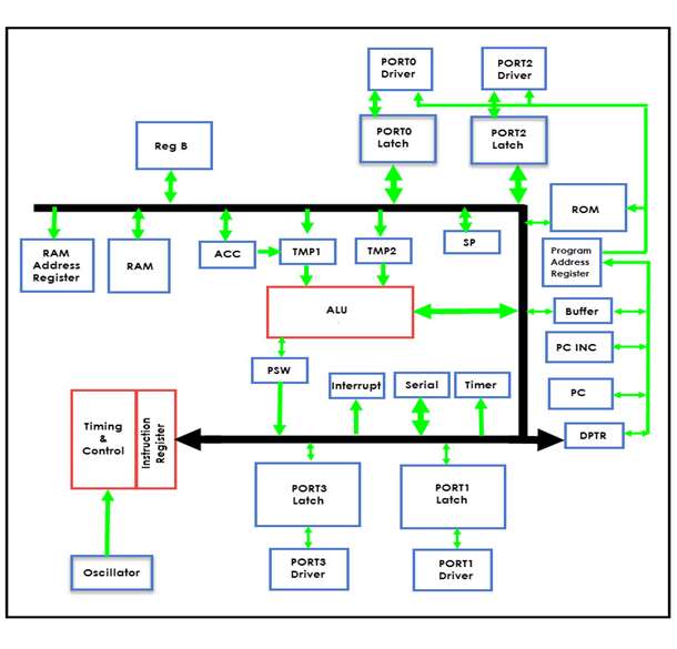
- Program status word (PSW): This register contains information about the status of the program. The PSW register has several bits that reflects the current status of the CPU.
- Program counter (PC): The program counter points to the address of the next instruction to be Executed. The program counter is 16 bits wide.
- Data pointer (DPTR): The data pointer is 16 bit register. It is used to hold the address of the data in the memory.
- Stack pointer (SP): The stack is a section of RAM used by the CPU to store information temporarily. This information could be data or an address. The register used to access the stack is called the SP register. The stack pointer in the 8051 is only 8 bit wide.
- Memory: Micro controller requires a program which is a collection of instructions. This program tells micro controller to do specific tasks. These programs require a memory, which is used to store the program of the micro controller is known as Program memory. It is known as ROM memory to store data or operands temporarily of the micro controller. The data memory of the 8051 is used to store data temporarily for operation is known RAM memory.
- Interrupts: Interrupts is a sub-routine call that given by the microcontroller when some other program with high priority is request for acquiring the system buses the n interrupts occur in current running program.
- Oscillator: As the micro controller is digital circuit therefore it needs timer for their operation. To perform timer operation inside micro controller it required externally connected or on-chip oscillator is used inside microcontroller.
- BUS : Basically Bus is a collection of wires which work as a communication channel or medium for transfer of Data. Here two types of buses that are shown in below,Address Bus: 8051 microcontrollers is consisting of 16 bit address bus. It is generally be used for transferring the data from Central Processing Unit to Memory. Data bus: 8051 micro controller is consisting of 8 bits data bus. It is generally be used for transferring the data from one peripherals position to other peripherals.
- Timing & Control unit: This unit derives all the necessary timing and control signal required for the internal operation of the circuit. It also derives control signals required for controlling the external system bus.
- Port 0 to Port 3 Latches & Drivers: These four latches and driver pairs are allotted to each of the four on chip I/O ports. These are identified as P0, P1, P2, P3.
3. Explain the PSW register of 8051 and show it contents?
The program status word (PSW) register is an 8-bit register. It is also referred to as the flag register. Although the PSW register is 8 bits wide, only 6 bits of it are used by the 8051. The two unused bits are user-definable flags. Four of the flags are called conditional flags, meaning that they indicate some conditions that result after an instruction is executed. These four are CY (carry), AC (auxiliary carry), P (parity), and OV (overflow).
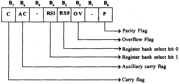
- CY, the carry flag: This flag is set whenever there is a carry out from the D7 bit. This flag bit is affected after an 8-bit addition or subtraction. It can also be set to 1 or 0 directly
- P, the parity flag: The parity flag reflects the number of 1 s in the A (accumulator) register only. If the A register contains an odd number of Is, then P = 1. Therefore, P = 0 if A has an even number of Is.
- OV, the overflow flag: This flag is set whenever the result of a signed number operation is too large, causing the high-order bit to overflow into the sign bit. The overflow flag is only used to detect errors in signed arithmetic operations.
4. Define interrupts in 8051 micro controller?
Interrupts are the events that temporarily suspend the main program, pass the control to the external sources and execute their task. It then passes the control to the main program where it had left off. The 8051 micro controller have five different events that cause the main program to interrupt from the normal execution. These five sources of interrupts in 8051are:
- Timer 0 overflow interrupt- TF0
- Timer 1 overflow interrupt- TF1
- External hardware interrupt- INT0
- External hardware interrupt- INT1
- Serial communication interrupt- RI/TI
5. Name the two register associated with the interrupt handling? (2)
IE (Interrupt Enable) Register, IP (Interrupt Priority) Register, TCON Register.
6. State the capacity of internal RAM in 8051 Micro controller? (2)
The 8051 has only 128-bytes of internal RAM. So if we want to expand the RAM memory, we have to use the external RAMs with proper addressing schemes.
7. Draw the internal architecture of 8051?(6)
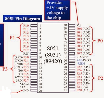
8. Draw the Pin diagram of 8051?
2 – unit
- Explain with examples any two addressing modes in 8051? OR Explain with examples any two addressing modes in 8051?
1. Immediate addressing mode: In this type, the operand is specified in the instruction along with the opcode. In simple way, it means data is provided in instruction itself.Ex: MOV A,#05H – Where MOV stands for move, # represents immediate data. 05h is the data. It means the immediate date 05h provided in instruction is moved into A register.
2.Register addressing mode: Here the operand in contained in the specific register of micro controller. The user must provide the name of register from where the operand/data need to be fetched. The permitted registers are A, R7-R0 of each register bank.Ex: MOV A,R0-> content of R0 register is copied into Accumulator.
3. Direct addressing mode: In this mode the direct address of memory location is provided in instruction to fetch the operand. Only internal RAM and SFR’s address can be used in this type of instruction.
Ex: MOV A, 30H => Content of RAM address 30H is copied into Accumulator.
4. Register Indirect addressing mode: Here the address of memory location is indirectly provided by a register. The ‘@’ sign indicates that the register holds the address of memory location i.e. fetch the content of memory location whose address is provided in register.
Ex: MOV A,@R0 => Copy the content of memory location whose address is given in R0 register.
2. Write any four logical operations of 8051 with example?
Logical operations in 8051 perform bitwise operations between the accumulator and data stored in a memory location, register, or data given by the programmer. The result of a logical operation is stored in the accumulator itself.Operations – example ,
- AND – ANL A, #data
- OR – ORL A, #data
- NOT – CPL A
- XOR – XRL A, #data
3. Describe the instruction set of 8051 microcontroller? OR Describe arithmetic operations in 8051?
The 8051 instruction set is divided into 4 functional groups,
- Arithmetic:
Addition:
- ADD – 8-bit addition between the accumulator (A) and a second operand. The result is always in the accumulator. The CY flag is set/reset appropriately.
- ADDC (Add with carry) – 8-bit addition between the accumulator, a second operand and the previous value of the CY flag puts the result in A
- DA – Decimal adjust the accumulator, Format the accumulator into a proper 2 digit packed BCD number. Operates only on the accumulator. Works only after the ADD instruction.
Substraction:
- SUBB – Subtract with Borrow. Subtract an operand and the previous value of the borrow (carry) flag from the accumulator.
- DEC – Decrement the operand by one from the source operand and returns the result to the operand.
Multiplication: MUL performs the multiplication of the A register by the B register, returning a double byte result. MUL AB– Multiply A by B and place result in A
Division: DIV AB divides the unsigned eight-bit integer in the Accumulator by the unsigned eight-bit integer in register B. The Accumulator receives the integer part of the quotient; register B receives the integer remainder. The carry and OV flags are cleared.
- Logic:
- ANL – can be used to clear (0) certain bits
- ORL – can be used to set (1) certain bits
- CLR A – All bits in register A are cleared
- CPL A – All bits in register A are complemented (inverted) ,Note that CLR and CPL instructions operate on register A
- RL A – Rotates A one bit position to the left
- RLC A – Rotates A and the carry flag one bit position to the left
- RR A – Rotates A one bit position to the right
- RRC A – Rotates A and the carry flag one bit position to the right
3)Data Transfer:
- MOV – Performs a bit or byte transfer from the source operand to the destination operand.
- PUSH / POP – Push and Pop a data byte onto the stack. The data byte is identified by a direct address from the internal RAM locations.
- XCH: Exchanges the value of the Accumulator with the value contained in register.
- XCHD(Exchange Digit) – Exchange lower digit of accumulator with the lower digit of the memory location specified. XCHD A, @Ri
4)Control Transfer: There are 3 classes of operations.
- Unconditional calls, returns & jumps
- Conditional Jumps
- Interrupt returns
- Unconditional Jump: Transfer control unconditionally to a new address.
- LJMP 16 bit address – LJMP is used to jump to any address location within 64KB code memory space of the 8051.
- SJMP (Short jump) – This is a 2 –byte instruction the first byte is opcode and the second byte is a singed number displacement, which is added with the PC of the instruction following the SJMP to get the target address.
- AJMP (Absolute jump) – It transfer the program execution to the target address unconditionally the target address for this instruction must be with in 2K byte memory.
4. Distinguish between XCH & XCHD instructions in 8051?
XCH: Exchanges the value of the Accumulator with the value contained in register. e.g. XCH A, R0 – exchanges the value between A and R0
XCHD (Exchange Digit) – Exchange lower digit of accumulator with the lower digit of the memory location specified. XCHD A, @Ri
5. Explain the difference between JUMP and CALL instructions in 8051?
| JUMP Instruction | CALL instruction |
| By using JUMP, the program control transfers to a location which is also a part of the main program | By using CALL instruction, the program control transfers to a location which is not a part of main program. |
| Here the addressing mode is Immediate | Here the addressing mode is Immediate and Register Indirect. |
| We do not need to initialize the Stack Pointer (SP) to perform the JUMP instruction. | We have to initialize the Stack Pointer (SP) before using some CALL instruction. |
| The program counter value is not Pushed into Stack | The value of program counter is pushed into stack before going to the pointed location. |
| No return instruction is needed after JUMP instruction. | After CALL, it enters into a subroutine, to come back from subroutine we need return instruction. |
| The value of stack pointer remain unchanged | The value of Stack Pointer is decremented by 2. |
6. Write the syntax of the instruction used to perform division operation in 8051 micro controller?
- MOV A, #data1
- MOV F0, #data2
- DIV AB
- MOV R0, A (Quotient)
- MOV R1,F0 (Remainder)
- RET
3 unit
- List the basic features of PIC 18?(6)
- It is 8-bit Microcontroller.
- It has 16-bit Instruction sets.
- 256 byte of EPROM.
- 2 KB SRAM.
- It can be set accept level triggered or edge triggered inputs.
- It can handle 8 external interrupts.
- It has 10-bit A/D Converter.
- It supports Instruction Pipelining.
- It is implemented with nano watt Technology (low power consumption ).
2. Describe PIC (Programmable Interrupt Controller )architecture?
Programmable Interrupt Controller is used when several I/O devices transfer data using interrupt and they are to be connected to the same level of the microprocessor.
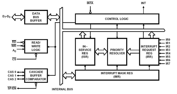
| Data Bus Buffer | This block is used to communicate between 8259 and 8085/8086 by acting as buffer. It takes the control word from 8085/8086 and send it to the 8259. It transfers the opcode of the selected interrupts and address of ISR to the other connected microprocessor. It can send maximum 8-bit at a time. |
| R/W Control Logic | This block works when the value of pin CS is 0. This block is used to flow the data depending upon the inputs of RD and WR. These are active low pins for read and write. |
| Control Logic | It controls the functionality of each block. It has pin called INTR. This is connected to other microprocessors for taking the interrupt request. The INT pin is used to give the output. If 8259 is enabled, and also the interrupt flags of other microprocessors are high then this causes the value of the output INT pin high, and in this way this chip can responds requests made by other microprocessors. |
| Interrupt Request Register | It stores all interrupt level that are requesting for interrupt service. |
| Interrupt Service Register | It stores interrupt level that are currently being execute. |
| Interrupt Mask Register | It stores interrupt level that will be masked, by storing the masking bits of interrupt level. |
| Priority Resolver | It checks all three registers, and set the priority of the interrupts. Interrupt with the highest priority is set in the ISR register. It also reset the interrupt level which is already been serviced in the IRR. |
| Cascade Buffer | To increase number of interrupt pin, we can cascade more number of pins, by using cascade buffer. When we are going to increase the interrupt capability, CSA lines are used to control multiple interrupts. |
3. Identify two types of serial communication?
Asynchronous and Synchronous serial communication
4. Describe between asynchronous and synchronous serial communication?
SYNCHRONOUS: Transfer the block of data (characters) between sender and receiver spaced by fixed time interval. This transmission is synchronized by an external clock. Faster transfer and less overhead.
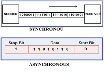
ASYNCHRONOUS: There is no clock involved here and transmission is synchronized by special signals along the transmission medium. It transfers a single byte at a time between sender and receiver along with inserting a start bit before each data character and a stop bit at its termination so that to inform the receiver where the data begins and ends.
5. Define half duplex and full duplex?
Half-duplex means data will be transmitted in both directions but at one time, only one device can transmit.
Full-duplex means data may be transmitted in both directions at one time, while one device is transmitting, it can also receive data transmitted from other devices at same time.
6. Write the three modes of 8255 PPI?
- Input/ Output Mode.
- Bit Set Reset (BSR) Mode.
6. Explain AVR architecture with a block diagram?
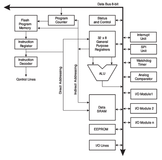
Data BUS 8 bit: Its an 8-bit parallel data lines by which the data travels inside the MCU (NOTE: this is the reason why AVR is an 8-bit MCU).
ALU: Arithmetic Logic Unit, the core/heart of the entire system where typically all commands get executed.
Data SRAM: It basically pretty similar to the RAM (Random access memory) we see inside our computers.
EEPROM: (Electrically Erasable Programmable Read Only Memory) its very similar to another component in our computer namely HardDisk, i.e. a permanent storage.
I/O lines: These are the bunch of registers which is used as a switches or controls for different features of AVR.
32X8 GPR (General Purpose Registers): This are 32 registers each having 8-bit which is a general storage space for data. But, remember, SRAM is also a temporary storage but these registers have some specialty among all.
Status & Control: A couple of registers which are very special to the MCU & to us also.
Program Counter: This is a register which has a responsibility to track the position of the program that is currently executing.
Flash Memory: It is also a permanent storage but its only for storing the program we write to it
7. Write any four features of AVR microcontroller?
- This module performs numerous functions that have two-directional inputs and output ports which can be configured with the pull-up resistances.
- There are numerous inner oscillators, consisting of RC oscillators also exits on this board.
- Internal data EEPROM up to 4 KB
- Internal SRAM up to 16 KB
- Multiple power-saving sleep modes
- Lighting and motor control (PWM-specific) controller models
- There is a flash memory of 250 kilobyte storage space exits on this board.
- The static random access memory having space of sixteen kilobytes is exist on this board.
- There are 2 timers of eight bit and sixteen-bit exits on this board.
- The pulse width modulation output exists on this board.
- There is an analog comparator also assembled on this module
8. What is a PPI?
Programmable peripheral interface, it is a multipoint input / output device. It is a general purpose device for interfacing parallel I/O devices to microprocessor/microcontroller bus.
9. Draw the block diagram of 8255 Programmable Peripheral Interface?
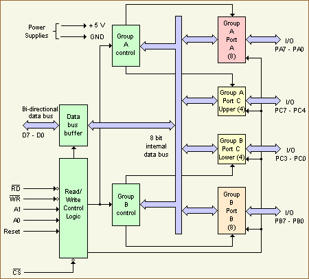
The parallel input-output port chip 8255 is also called as programmable peripheral input- output port. It has 24 input/output lines which may be individually programmed in three groups of eight lines. The two groups of I/O pins are named as Group A and Group B. Each of these two groups contains a subgroup of eight I/O lines called as 8-bit port and another subgroup of four lines or a 4-bit port.
Thus Group A contains an 8-bit port A along with a 4-bit port C upper. The port A lines are identified by symbols PA0-PA7 while the port C lines are identified as PC4-PC7. Similarly, Group B contains an 8-bit port B, containing lines PB0-PB7 and a 4-bit port C with lower bits PC0- PC3. The port C upper and port C lower can be used in combination as an 8-bit port C. Both the port C are assigned the same address. Thus one may have either three 8-bit I/O ports or two 8-bit and two 4-bit ports from 8255. All of these ports can function independently either as input or as output ports. This can be achieved by programming the bits of an internal register of 8255 called as control word register (CWR). This buffer receives or transmits data upon the execution of input or output instructions by the microprocessor. The control words or status information is also transferred through the buffer.
- RD: This is the input line driven by the microprocessor and should be low to indicate read operationto 8255.
- WR: This is an input line driven by the microprocessor. A low on this line indicates write operation.
- CS: This is a chip select line. If this line goes low, it enables the 8255 to respond to RD and WRsignals, otherwise RD and WR signal are neglected.
- A1-A0: These are the address input lines and are driven by the microprocessor. These lines A1-A0with RD, WR and CS from the following operations for 8255. These address lines are used for addressing any one of the four registers
- D0-D7: These are the data bus lines those carry data or control word to/from the microprocessor.
- RESET: A logic high on this line clears the control word register of 8255. All ports are set as inputports by default after reset.
10. Identify any two applications of PLC?
- Process Automation Plants (e.g. mining, oil &gas)
- Glass Industry
- Paper Industry
- Cement Manufacturing
- In boilers – Thermal Power Plants
4- Unit
- Define asynchronous serial communication?
Asynchronous serial communication is a form of serial communication in which the communicating endpoints’ interfaces are not continuously synchronized by a common clock signal.
- Construct block diagram of PLC?
PLC stands for programmable logic control is microprocessor based programming technique. It controls the different process and is programmed according to the operational requirement of that process.
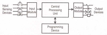
It consists of following basic parts,
- CPU
- Programming device
- Input & output module


Recent Comments