
Diode Characteristics
DIODE CHARACTERISTICS
AIM
- To obtain the forward & reverse characteristics of a Si diode (1N4001). Also to find the static & dynamic forward resistances.
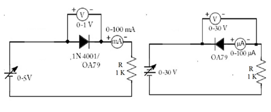
- To obtain the forward & reverse characteristics of a Ge diode (0A79). Also to find the static & dynamic forward & reverse resistances.
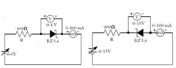
- To obtain the forward & reverse characteristics of a Zener diode (BZ 5.6). Also to find the static & dynamic forward & reverse resistances.
COMPONENTS REQUIRED
- DC Power Supply − 0-5V, 0-30V, 0-15V
- Ammeter – 0-100mA, 0-100µA
- Voltmeter – 0-1V, 0-30V, 0-15V
- Resistors – 1kΩ
- Diodes – 1N4001, 0A79, BZ 5.6
- CRO
- Miscellaneous –Probes, Connecting wires, Breadboard, etc.
THEORY
When a p-type & n-type semiconductors are joined together, a pn-junction diode with a unique ability of permitting current in one direction is formed. The lead connecting p-type semiconductor is called anode & that to the n-type semiconductor is called as cathode. Before the formation of junction the semiconductors are electrically neutral, but on junction formation due to concentration gradient of electrons & holes majority carriers try to diffuse through the junction. This diffusion ends in neutrality and forms a potential barrier across the junction. This barrier region is devoid of majority carriers and is known as depletion region & extends to a depth of 1µm. The potential across this depletion region is known as barrier potential. In case, of Si diode its value is 0.7V and for Ge diode it has a value 0.3V.
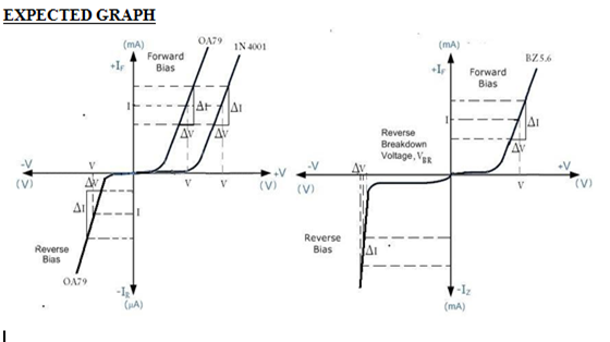
If the anode & cathode of the diode are connected to the positive & negative terminals of a power supply resp. then the diode is said to be under forward biased condition. Untill the supply overcomes the barrier potential value no current flows through the diode. On overcoming, the barrier potential current (in the range of mA) starts to flow through the diode.
If the cathode & anode of the diode are connected to the positive & negative terminals of a power supply resp. then the diode is said to be under reverse biased condition. Under this condition the depletion region at the junction widens and no majority carriers pass through it. But the minority charge carriers cross across the junction and a very small current known as reverse leakage current,( In case, of Si diode- nA order and for Ge diode- µA order), starts to flow through the diode.
Zener diodes are specially designed one’s which is capable to operate in the reverse breakdown region without causing any damage. This feature of zener diode is achieved by heavy doping which results in narrow depletion region. Under forward bias condition, the diode behaves as that of normal Si diode with a forward voltage drop of 0.7V. Under high reverse bias condition, voltage greater than diode’s reverse breakdown voltage, the charge carriers in the depletion region are pulled out from covalent bonds creating electron-hole pairs thereby resulting in high reverse current flow. This phenomenon is known as zener breakdown. If the reverse bias voltage if further increased, the voltage drop across the diode remains constant but current flowing increases. All type of diodes possess two types of resistances. ie;
Static/DC resistance- It’s the ratio of DC voltage across the diode to the current flowing through the diodeat that instant.
Static resistance= Voltage/ Current
CIRCUIT DIAGRAM
TABULATION
PROCEDURE
- Identify the leads of the given diodes and check their working condition.
- Setup the circuit for performing the forward characteristics of Si diode.
- Vary the DC supply voltage in steps of 0.1V and note the corresponding ammeter and voltmeter readings and enter in the tabular column. Continue the tabulation till the voltmeter reads 0.8V-0.9V.
- Repeat the above procedure by replacing Si diode with Ge & zener diodes.
- Setup the circuit for performing the reverse characteristics of Ge diode.
- Vary the DC supply voltage in steps of 1V and note the corresponding ammeter and voltmeter readings and enter in the tabular column. Continue the tabulation till sufficient data has been obtained.
- Repeat the above procedure by replacing Ge diode with zener diode.
- Plot the V-I characteristics of Si, Ge & zener diode, using the data in corresponding tabular column.
- Calculate the forward & reverse static resistance & dynamic resistance values using the graphs plotted.
EXPECTED GRAPH


Recent Comments