
Transistor Characteristics lab manual
TRANSISTOR CE CHARACTERISTICS
AIM
To study and plot the input & output characteristics of a NPN transistor in CE configuration. Also to find the following parameters.
- Input impedance, ri
- Output impedance, ro
- Forward Current gain, β
COMPONENTS REQUIRED
- Transistor – BC 107/BC 547/ SL 100
- Resistors – 100Ω
- DC power supply – 0-5V, 0-30V
- Voltmeter – 0-1V, 0-30V
- Ammeter – 0-100µA, 0-100mA
- Miscellaneous – Breadboard, Connecting wires, etc.
THEORY
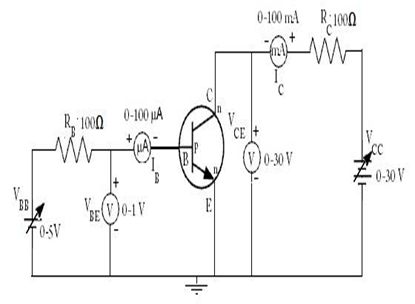
In this configuration, input is applied between the base & emitter and the output is taken from collector & emitter. The emitter of the transistor is common to both input & output ports and hence its named as Common Emitter (CE) configuration.Common emitter is most frequently used configuration for amplification because it provides voltage, current & power gains more than unity and it also has moderate values for input & output impedances.
Input Impedance, ri
It is the ratio of change in base-emitter voltage, (∆VBE) to the change in base current (∆IB) at constant output voltage, VCE ie,
Output Impedance, ro
It is the ratio of change in collector-emitter voltage, (∆VCE) to the change in collector current (∆IC) at constant input current, IB ie,
Forward Current Gain, β
It is the ratio of change in collector current to the corresponding change in base current, keeping the output voltage, VCE as a constant ie,
CIRCUIT DIAGRAM
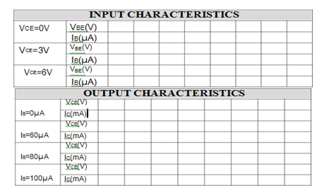
TABULATION
PROCEDURE
Input Characteristics
- Identify the leads of the given NPN transistor and check the transistor using multimeter.
- Setup the circuit as shown in the figure & verify the connections using multimeter.
- Switch ON the power supplies keeping VBB at minimum position & VCE at 0V.
- Note down the value of IB for different values of VBE by varying VBB from 0V to 0.8V/0.9V in steps of 0.1V and enter them in the tabular column.
- Repeat the above step for VCE say 3V & 6V.
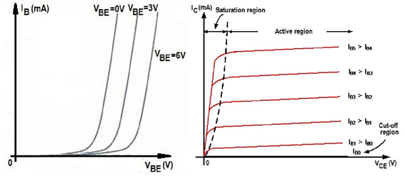
- Plot the input characteristics on graph sheet using the data tabulated with VBE on x-axis & IB on y-axis.
- Calculate dynamic input resistance value from the graph plotted.
Output Characteristics
- Switch ON the power supplies keeping VCC at minimum position & IB at 0µA.
- Note down the value of IC for different values of VCE by varying VCC from 0V to 10V/15V in steps of 0.5V and enter them in the tabular column.
- Repeat the above step for IB say 60µA, 80µA & 100µA.
- Plot the output characteristics on graph sheet using the data tabulated with VCE on x-axis & IC on y-axis.
- Calculate dynamic output resistance & forward current gain from the graph plotted.
EXPECTED GRAPH
CE input & output characteristics


Recent Comments