
Full wave rectifier circuits Lab Manual
Full wave rectifier circuits (Centre tapped)
Aim:
To study the characteristics of Full wave rectifier with and without filter and calculate its ripple factor.
Components and equipments required:
- Diode 1N4007 2no
- Resistor 1K 1no
- Step down transformer 6-0-6 1no
- Breadboard, CRO, BNC probe, connecting wires etc….
Theory:
Rectifier is a circuit used to convert AC to DC The diode conducts only when its anode is at a higher voltage with respect to cathode.
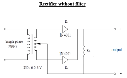
- Full wave circuit comprise of two half wave circuits which are so connected that conduction takes place through one diode during one half of the power cycle and through the other diode during the second half of the power cycle. The current to the load which is the sum of these two currents conducted by the diodes at each half cycle. The peak inverse voltage in this case is 2Vm.
- Full wave circuit consist of an ac voltage source, step down transformer, Two single pn junction diode and load.
- During positive half cycle-secondary winding of center tapped transformer. The positive voltage at point diode D1 to conduct as it is forward biased. At the same time the negative voltage at D2 makes to diode remain off as it is reverse biased.
- During positive half cycle of input, diode D1, conducts and diode D2 does not conduct. The current flows through the diode D1, load resistor RL and the upper half of the winding Hence, the voltage drop across RL will be equal to the input voltage.
- During the negative half cycle of the input, the diode D2 positive and Diode D1 is negative. The diode D1, to remain off and positive voltage appearing at point D2 makes the diode D2 to conduct. So during negative half cycle of input, diode D1 does not conduct and diode D2 conducts.
- The current flows through the diode D2 load resistor RL and the lower half of the winding.
- The voltage drop across RL will be equal to the input voltage. The currents i1 and i2 flows through the load RL in the same direction.
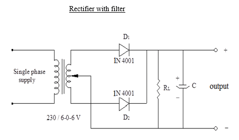
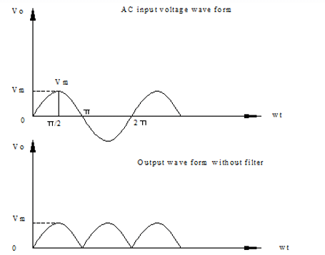
- The output is not a steady dc but only a pulsating dc wave. it has a dc value, called ripples.To eliminate the dc components in the output, by using filter circuit. Hence the circuits that converts a pulsating output from a rectifier to a very steady dc level is known as filter.
- The main function of a filter circuit is to minimize the ripple content in the rectifier output. Certain electronic circuits need smooth DC voltage.
- Vdc = 2 Vm/Π = 0.636 Vm
- Vrms = 0.707 Vm
- Form factor =rms value/average value = 1.11
- PIV (Peak inverse voltage) = 2 Vm
- Ripple factor = 0.482
- Efficiency = 81.2 %
Procedure:
- The circuit is wired as in the circuit diagram.
- Connect the supply voltage to the primary of the centre-tapped transformer.
- Connect the output terminals to the CRO and observe the input- output waveform.
- Switch On mains supply. Observe the transformer secondary voltage waveform and output voltage waveform across the load resistor, simultaneously on the CRO screen. Note down the peak values.
- Measure the DC voltage across the load resistor.
- Calculate the ripple factor and DC output voltage. Compare practical and theoretical results.
Circuit Diagram
Wave Form
Result :
Ripple factor , r = (with filter)


Recent Comments