
Power Electronics Lab Manual
Experiment No: 1
STATIC V-I CHARACTERISTICS OF SCR
AIM:
To plot the static V-I characteristics of the given SCR.
EQUIPMENTS AND COMPONENTS REQUIRED:
| Sl No | Equipment/Component | Specification | Quantity |
| 1 | SCR- | ||
| 2 | Ammeters- | ||
| 3 | Power Supply- | ||
| 4 | Wattage Resistors- | ||
| 5 | Voltmeters- |
THEORY:
A silicon controlled rectifier (SCR) is the oldest and most widely used member of the thyristor family. The SCR is a four layer pn-pn device with three junctions. It has three terminals: anode, cathode and gate. The SCR is used essentially as a controlled switch,. Fast switching action, small size, high reliability, low loss, high current and high voltage ratings are the useful features which make the SCR suitable for power control in many applications.
The static V-I characteristics of an SCR is shown in figure. The SCR has three modes of operation: reverse blocking mode, forward blocking mode (off state) and forward conduction mode (on state).
CIRCUIT DIAGRAM:
| VAK (V) | IA (µA) |
OBSERVATIONS:
Reverse Blocking Mode:
When the cathode is positive with respect to the anode, the junctions J1 and J3 are reverse biased and J2 is forward biased. Only a small leakage current of the order of a few milli-amperes or micro-amperes flows and the device is in the reverse blocking mode. When the voltage is increased to the reverse breakdown voltage, the depletion layers at the junctions J1 and J3 breakdown and the current through the device increases to a high value.The high current at high voltage causes more losses in the device and the junction temperature may exceed the permissible value resulting in the damage of the device.
Forward Blocking Mode:
When the anodeis made positive with respect to thecathode, J1 and J3 are forward biased and J2 is reverse biased. The reverse biased junction J2limits the anode current to a few milli-amperes (forward leakage current). The SCR is then said to be in the forward blocking mode. Application of a small positive gate current causes slight increase of forward leakage current.
Forward conduction mode:
When the SCR is in the forward blocking mode, if the anode to cathode voltage is increased to the forward breakdown voltage, junction J2 breaks down so that the SCR becomes equivalent to a conducting diode. The voltage across the device falls to a small value and the anode current is limited by the load impedance. When theforwardvoltage is less than the forward breakdown voltage, the SCR can be triggered into conduction by applying a pulse of positive gate current. Lower anode to cathode voltage requires higher gate trigger current and higher anode to cathode voltage requires lower gate trigger current. If the gate current is sufficiently large, the device can be turned on with a small anode to cathode voltage.
PROCEDURE:
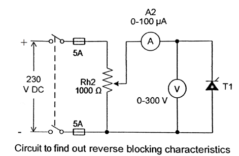
Reverse Blocking Characteristics:
Connections are made as in figure (i). Keeping the potential divider in its minimum position, 230V supply is switched on. The cathode to anode voltage is gradually increased and the ammeter and voltmeter readings are noted.
CIRCUIT DIAGRAM:
Observations:
| Ig = 0 | Ig = 0.5 Igt | ||
| VAK(V) | IA (µA) | VAK(V) | IA (µA) |
CIRCUIT DIAGRAM:
Observations:-
| VAK (V) | IA (A) |
Determination of Vgt and Igt:
To obtain the values of the minimum values of gate voltage (Vgt) and gate current (Igt) to turn on the thyristor, connections are made as in fig(ii). Keeping the anode resistance RA at its maximum position and the voltage applied to the gate zero (i.e., potential divider RG at its minimum position), the 30V power supply is switched on. With zero gate voltage, the thyristor is in the forward blocking mode. The gate voltage is gradually increased, till the anode current suddenly increase.The gate voltage and gate current corresponding to this point give Vgt and Igt.
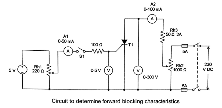
Forward Blocking Characteristics:
Connections are made as in fig(iii). Keeping the series resistance maximum and potential divider in its minimum position, 230V supply is switched on. Keeping gate circuit open, the anode to cathode voltage is gradually increased and the ammeter and voltmeter readings are noted. Now the key K1 is closed and gate voltage is adjusted to get 0.5 Igtandprocedure is repeated.
ForwardConduction Characteristics:
Connections are made as in fig(iv). The gate voltage is adjusted to get sufficient gate voltage to turn on the SCR. Now 30V supply is switched on keeping the anode resistance at its maximum value and key K2 open. After ensuring that the SCR is conducting, the key K2 is closed. The anode current and anode to cathode voltage are noted. The anode current is increased in steps and anode to cathode voltage is noted in each case.
RESULTS:
Experiment No: 2
R AND RC TRIGGERING CIRCUITS
AIM:
To design and setup R and RC triggering circuits for a half controlled rectifier for different firing angles and draw relevant waveforms.
APPARATUS REQUIRED:
| Sl No | Apparatus/Tool | Specification | Quantity |
| 1 | SCR- | ||
| 2 | Ammeters- | ||
| 3 | Power Supply- | ||
| 4 | Wattage Resistors- | ||
| 5 | Voltmeters- | ||
| 6 | Potentiometers | ||
| 7 | Capacitor | ||
| 8 | SCR | ||
| 9 | Transformer | ||
| 10 | Bread Board |
THEORY:
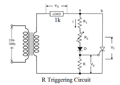
R Firing circuit:
Figure shows the most basic circuit. R2 is the variable resistance. Rb is the stabilizing resistance. If R2 is zero, gate current may flow from source through R1, D and gate to cathode. This current should not exceed maximum permissible gate current Igm. R1 can therefore be found from the relation (Vm/R1) ≤ Igm. The function of R1 is to limit gate current to a safe value, as R2 is varied. Resistance Rb should have such value that maximum voltage drop across it does not exceed maximum possible gate voltage Vg. This happens only when R2 is zero. Under these condition . As resistances R1, R2 are large, gate trigger circuits draw a small current. Diode D allows the flow of current during the positive half cycle only i.e., gate voltage is half wave DC pulse. The amplitude of this DC pulse can be controlled by varying R2. The potentiometer setting R2 determines the gate voltage amplitude. When R2 is large, current I is small and voltage across Rb is Vg = I x Rb. As Vg is less than Vgt SCR will not turn on. Trigger circuit consists of resistance only. Vg is therefore inphase with source voltage Vs. Adjust R2 in such a way that Vg = Vgt at different firing angles depending upon instantaneous values of input voltage. When R2 is large enough to such that Vg become equal to Vgt only at peak value of output voltage, corresponding firing angle will be 900. The resistance triggering cannot give firing angle beyond 900.
Circuit Diagram:
Design:
When R2 is minimum, Ig will be maximum.
Igmax = 100 mA
Therefore = 170 Ω. (Use 220Ωstd.)
When R2 is maximum, current will be minimum and voltage drop across Rb will be maximum and it should not exceed Vgm
Vgmax = 2.5 V, Vm = 12√2 V
When R2 = Max
Vgt = 0.8 V, Vm = 12√2 V
R2 = 0.447 Ω (Use 1K pot std)
Sample Waveforms:
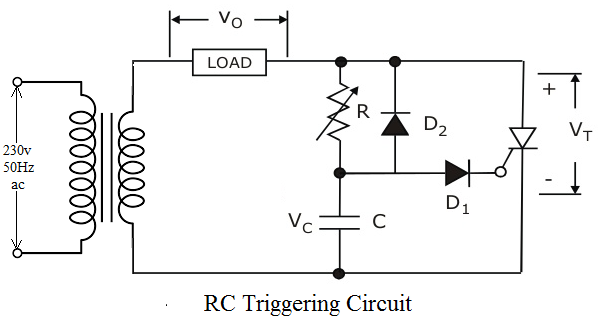
RC Firing circuit:
Fig.2 shows the RC half wave triggering circuit. By varying the value of R, firing angle can be controlled from 00 to 1800. In the negative half cycle capacitor C charges through D2 with lower plate positive to peak supply voltage Vm at ωt = 900. During the period ωt = -900 to ωt = 00, Vc may fall from –Vm at ωt = 900 to some lower value at ωt = 900. As the SCR anode voltage passes through zero and becomes positive C begins to charge through variable resistance R from initial voltage. When the capacitor charges to positive voltage equal to Vgt, SCR is fused and after this capacitor holds to small positive voltage. D1 is used to prevent breakdown of cathode to gate through D2 during negative half cycle. The SCR will trigger when Vc= Vgt+ Vd. At the instant of triggering VC is assumed constant. Hence the maximum value of R is given by
When the SCR triggers, voltage drop across it falls to 1 to 1.5V. This in turn lowers the voltage drop across R and C to this low value of 1 to 1.5V. Low voltage across SCR during conduction period keeps C discharged.
Circuit Diagram:
DESIGN:
Consider maximum firing angle to be achieved as 1600.
Vs = Vm Sin 1600 = 12√2 Sin 1600.
Igt = 200 µA
Vgt = 0.8 V, Vd = 0.6V
R = 22 KΩ
T = 20*10-3ms
C = 0.56 µF (Use 1µF std)
Sample Waveforms:
PROCEDURE
Set up the circuit on breadboard. Turn on the SCR by adjusting triggering pulse. Note down the maximum and minimum firing angle. Observe the waveforms corresponding to each firing angle.
RESULT:
The circuit is setup and the waveforms for various firing angles are observed and plotted.
Experiment No: 3
DIGITAL TRIGGERING CIRCUIT
AIM:
To design and set up a digital triggering circuit, suitable for triggering a single phase half wave controlled rectifier.
EQUIPMENTS AND COMPONENTS REQUIRED:
| Sl No | Apparatus/Tool | Specification | Quantity |
| 1 | IC 741 | ||
| 2 | IC 74121 | ||
| 3 | Power Supply- | ||
| 4 | Resistors- | ||
| 5 | Diode | ||
| 6 | Potentiometers | ||
| 7 | Capacitors | ||
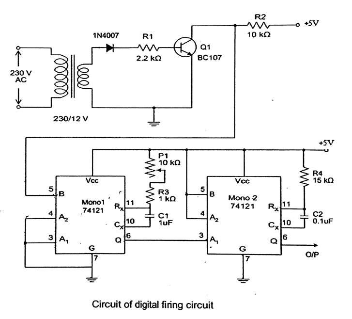
THEORY:
The actual firing circuit of a digital firing circuit suitable for triggering a single phase half wave controlled rectifier is shown in figure. The supply voltage is stepped down to an appropriate value and fed to the base of transistor Q1. The Transistor outputs a square wave in synchronism with the acc input. The square wave is fed to the monostable-1 (TTL IC 74121) which is positive edge triggered. At the positive going edgeoftheinput signal, the output of monostable-1 becomes high. Then after a time delay of Td1 = 0.7R1C1, the output of monostable-1 becomes low. Td1 can be varied from 0 to T/2 by varying the resistance R1. The output of monostable-1 is the triggering input to monostable-2, which is negativeedge triggered. So in every positive half cycle of the supply voltage, monostable-2 is triggered to the high state at a delay time of Td1. It is designed to remain in the high state for delay time Td2 which is sufficientto turn on the SCR. The output of monostable-2 is amplified and applied to the gate of SCR after isolation. By varying the resistance R1, the firing angle can be varied from 0 to 180o. In the pulse amplifier and isolation block, the transistor is for pulse amplification and the pulse transformer is for providing isolation between power circuit and firing control circuit. The diode placed across the secondary of the pulse transformer protects gate of the thyristor from large reverse voltages. The diode in series with the gate prevents any leakage current flowing in the gate circuit during transistor conduction. The diode placed across the primary of the pulse transformer protects the thyristor from over voltages.
Time delay of monostable-1 is given by
Td1 = 0.7R1C1
Maximum time delay,
Td1 (max) = 0.7R1maxC1
Since maximum time delay is 180o,
Td1 (max) = T/2, where T is the time period of the ac supply.
Thus,
R1max =
Width of output pulse Td2 of monostable-2 should be sufficient to turn on the SCR.
Td2 = 0.7R2C2
Thus,
R2 =
Suitable values of R1, C1, R2and C2are selected.
Design:
For Mono 1output,
T=0.7RC, Take C= 1μF
T(min) = 10ms
T(max) = 19ms
Rmin corresponding to 10ms, R=
RmaxCorresponding to 19ms, R=
Fix Rmin as fixed resistance and (Rmax –Rmin) as pot. Take15k resistor and 15k pot.
For Mono 2 , Assume T= 1ms and take C = 0.1μF, then
R=
Take R as pot
Sample Waveform:
PROCEDURE:
The circuit is set up, supply is switched on. Waveforms at different points are observed on the CRO. The firing angle is varied by varying the resistance R1. For different firing angles, the above waveforms are observed.
RESULT:
A digital firing circuit has been designed and set up for triggering a single phase half wave controlled rectifier.
Experiment No: 4
TRIGGER CIRCUIT USING RAMP CONTROL
AIM:
To design and set up a ramp controlled trigger circuit for a thyristor in a single phase half wave controlled rectifier.
THEORY
For phase controlled rectifier, the trigger pulse must be synchronized with the main supply. In ramp control circuit, the ramp generator produces a saw tooth waveform in synchronism with main supply. This ramp is compared with a DC level in an opamp comparator. The output of the comparator is the trigger pulse which may be directly applied or through one amplifier and pulse transformer to the thyristor gate. The trigger delay can be varied by varying the dc level applied to the comparator.
ZCD: The closed loop gain of the op-amp is selected high to get a square wave as output when the input signal crosses zero.
CIRCUIT DIAGRAM:
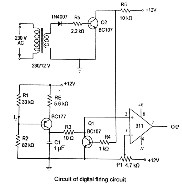
DESIGN:
Assume the value of capacitor as 1 .
The capacitor is charged at a constant current. Then the capacitor voltage will rise according to the expression.
Assume maximum voltage as 5v at 10ms, then,
I=
Assume emitter resistance voltage as about 3V. Then,
RE= , Take RE as 5.6
With RE=5.6 , VRE=
Assume I2 = 0.1mA, the base current will be negligible when compared to I2
Also We have,
Then,
Take R1 =33 and R2 = 82
R1 =120-85 = 35
PROCEDURE: Design the ramp control circuit as per the design given above. Choose 0.5mA as the charging current of the capacitor C in the ramp generator. Set up the circuit and test the performance.
RESULT:
A ramp control trigger circuit for a thyristor in a single phase half wave controlled rectifier has been designed and set up.
Experiment No: 5
CHARACTERISTICS OF POWER MOSFET
AIM:
1. To obtain the output characteristics of a power MOSFET.
2. To obtain the transfer characteristics of power MOSFET
THEORY:
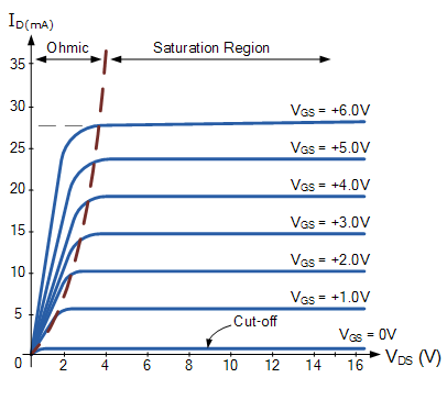
The power metal oxide semiconductor field effect transistor (MOSFET) is a device derived from the field effect transistor (FET) for the use as a fast acting switch at power levels. Unlike the bipolar transistor, which is a current controlled, the MOSFET is a voltage controlled device. The main terminals are the drain and source. The current flow from drain to source is being controlled by the gate to source voltage.
The absence of any stored charge makes very fast switching possible, with on and off times being much less than 1µs. Above approximately 100V, the conduction losses are higher for the bipolar transistor, but the switching loss is much less.
In the drain characteristics of the MOSFET, at very low values of drain source voltage, the device has a constant resistance characteristic but at higher values of drain source voltage, the gate voltage determines the current. However in power applications, the drain source voltage must be small in order to minimize the on state conduction losses.
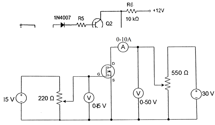
PROCEDURE:
Set up the circuits shown in figure.
Drain characteristics:Set up the circuit as shown in figure. Adjust the gate source voltage slightly above the threshold voltage (around 3 to 3.25 V). Keeping VGS constant, the variation of drain current with drain source voltage is noted. Repeat the experiment for different values of VGS.
Transfercharacteristics: Set up the circuit as shown in figure.Keeping VDS constant, the variation of drain current with gate source voltage is noted. Repeat the experiment for different values of VDS.(Dothe experiment for VDS=10 V and 12V).
CIRCUIT DIAGRAM:
SAMPLE WAVEFORM
OUTPUT CHARACTERISTICS TRANSFER CHARACTERISTICS
| VGS = 5V | VGS = 10V | ||
| ID(mA) | VDS (V) | ID(mA) | VDS (V) |
| VDS = 10V | VDS = 20V | ||
| VGS (V) | ID(mA) | VGS (V) | ID(mA) |
RESULT:
The drain characteristics and transfer characteristics of the given MOSFET are obtained.
Experiment No: 6
UJT FIRING CIRCUIT
AIM:
To design and set up a UJT firing circuit for a single phase half wave controlled rectifier or single phase ac regulator.
THEORY:
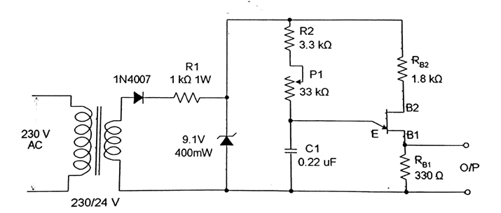
The UJT is atwo layer pn device with three terminals. The terminals are called emitter (E), base-1 (B1) and base-2 (B2). It consists of an n type silicon bar with ohmic contacts for the two base terminals. A single p type emitter junction is formed by alloying a p type material on the side of the silicon bar. Its structure, equivalent circuit and symbol are shown in figure (i).
Fig(i)
With positive voltage VBB applied between B1 andB2, the potential of point A with respect to B1 is given by
where η is called the intrinsic stand off ratio. Typical values of η range from 0.51 to 0.82 and RBB is of the order 5KΩ to 10KΩ.
The static emitter characteristic of a UJT is shown in figure (ii). When the emitter voltage is greater than VBB, the emitter – base1 junction becomes forward biased and the emitter current increases rapidly. Vd is the emitter diode drop (0.4 -0.7V).
Fig(ii)
Point A is called the peak point and the corresponding voltage and current are denoted by VP and IP. the forward biased pn junction produces large number of holes in the base1 region so that the resistance drops to a very low value (about 50Ω). As a result, voltage drop in R1 falls, the diode gets greater forward bias and the emitter current Ie increases as shown by portion AB of the characteristic. In the region AB, the device exhibits negative resistance, as an increase in emitter current is accompanied by a decrease in the emitter voltage. At point B, E-B1 region is saturated and R1 does not decrease any more. A further increase in Ieis accompanied by a rise in the emitter voltage as shown by the portion BC. Point B is called the valley point; VVandIV are the corresponding emitter voltage and emitter current. The negative resistance region between the peak point and the valley point gives the switching characteristic so useful in generating gate trigger signals for thyristor.
A synchronized UJT half wave trigger circuit is in figure. The output of the half wave diode rectifier is clipped to a standard level VZ by the zener diode. The voltage VZisappliedto the RC charging circuit. The capacitor charges at a rate determined by the charging resistor. When the capacitor voltage reaches the peak point emitter voltage, , the E-B1 junction of UJT breaks down. As a result, the capacitor discharges through the primary of the pulse transformer and a voltage pulse occurs at the secondary which is fed to the gate circuit of the thyristor of a half wave controlled rectifier or a single phase ac regulator. When the capacitor discharges the emitter circuit is turned off and the UJT is restored to its initial state. The capacitor charges again and similar operations repeat. The pulse repetition period is independent of the supply voltage and is given by . Slight variation in the pulse repetition frequency with temperature is compensated by the resistance Rb2 connected in series with base2. The value of Rb2 is given by .
Even though a number of pulses are produced in a half cycle, only the first pulse will determine the firing angle.
Since Vz goes to zero at the end of every half cycle, capacitor voltage falls to zero and begins to charge afresh at the beginning of every half cycle. So for a given value of R1, the time when the first pulse is applied to the SCR in a half cycle remains constant. The synchronization of trigger pulse with the supply voltage is thus achieved.
Changing the value of R changes the instant at which the first pulse occurs. So the firing angle can be controlled by varying R. The total range of control is around 150o. the charging resistor R must be sufficiently small to admit the required peak point current of the UJT.
or
Since
i.e.,
Again the resistance R must be sufficiently large so that the emitter current does not exceed the valley current IV.
or
The capacitor value should be such as to store sufficient charge to trigger the SCR. The typical values of C are 0.1 to 0.5µF. The value of the series resistance is calculated from
CIRCUIT DIAGRAM
SAMPLE WAVEFORMS:
DESIGN:
Thus C= µF
PROCEDURE:
The UJT trigger circuit is set up. The supply is stepped down to a suitable value to get the synchronizing signal, which is fed to the triggering circuit. The waveforms at various stages are observed on the CRO for different values of firing angle.
RESULT:
A UJT firing circuit for single phase half wave controlled rectifier (single phase ac regulator) has been designed, set up and the waveforms have been plotted.


Recent Comments